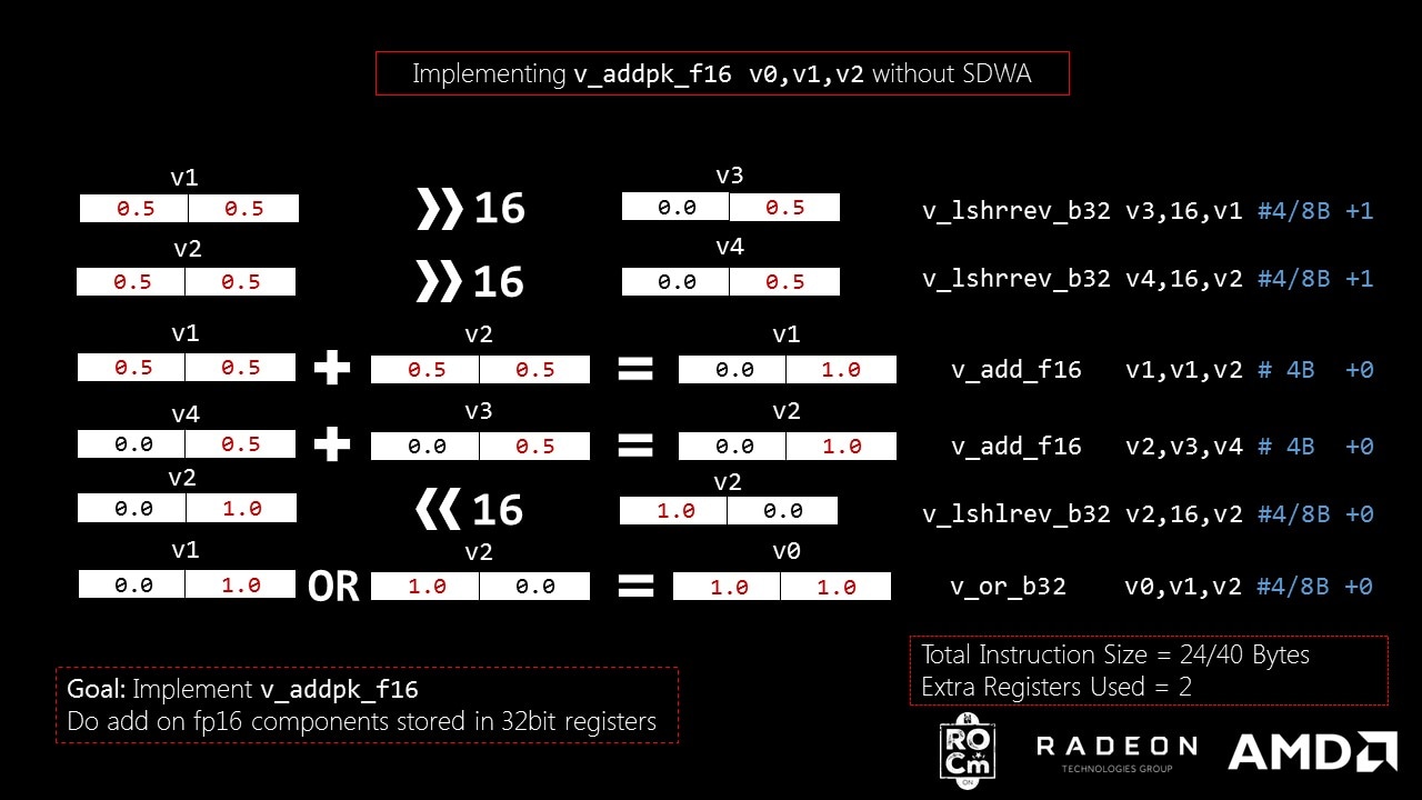
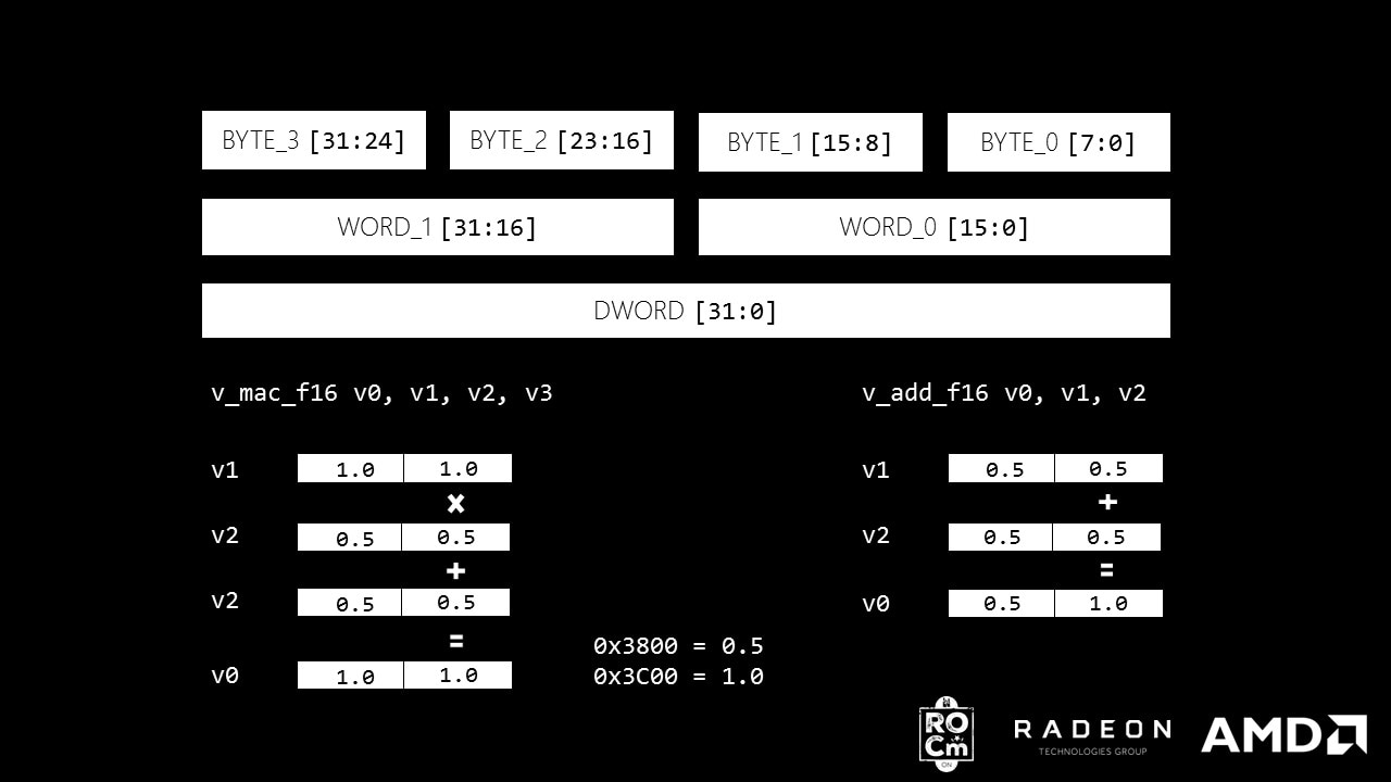
Sub DWord Addressing is a feature of the AMD GCN architecture which allows the efficient extraction of 8-bit and 16-bit values from a 32-bit register. Multiple small values can be packed into a 32-bit register, maximizing the utilization of a 32-bit register. Efficiently executing Sub DWord operations can be difficult, however. For example, to add two 16-bit floats (half) resident in the most significant ([31:16]) bits of 2 registers requires the programmer to shift the inputs, store the shifted values into a new register (this can cause register pressure), do a regular addition, shift the outputs back to the [31:16] bits and finally do a bitwise-OR on the final output.
The following code shows how this is implemented using GCN ISA (going forward in this blog, all comparisons are against ISA capabilities of GFX 8 Fiji + Polaris):
# Optimized for low register pressure
v_lshrrev_b32 v3, 16, v1 # can take 4 or 8 bytes
v_lshrrev_b32 v4, 16, v2 # can take 4 or 8 bytes
v_add_f16 v2, v3, v4 # can take 4 bytes
v_lshlrev_b32 v2, 16, v2 # can take 4 or 8 bytes
v_or_b32 v0, v1, v2 # can take 4 or 8 bytes
The compiler can generate between 20 and 36 bytes of binary for this section of the kernel. The performance is 1/5th the rate of a native 16-bit floating point add and uses 5 to 9 times the instruction cache of a native instruction. It also requires an extra 2 registers per code block.
We use the above code to implement v_addpk_f16
. v_addpk_f16
is packed addition on 16-bit floating point data present in a 32-bit register. For example, v_addpk_f16 v0, v1, v2
does v0.x = v1.x + v2.x
and v0.y = v1.y + v2.y
.
# Optimized for low register pressure
v_lshrrev_b32 v3, 16, v1 # can take 4 or 8 bytes
v_lshrrev_b32 v4, 16, v2 # can take 4 or 8 bytes
v_add_f16 v1, v1, v2 # can take 4 bytes
v_add_f16 v2, v3, v4 # can take 4 bytes
v_lshlrev_b32 v2, 16, v2 # can take 4 or 8 bytes
v_or_b32 v0, v1, v2 # can take 4 or 8 bytes
The code above shows how v_addpk_f16
can be implemented without SDWA. The code takes up 24 to 40 bytes of kernel binary and 2 extra registers are used. These short-comings can be solved by using Sub-DWord Addressing.
About Instruction Type
Sub-DWord Addressing (SDWA) is another instruction modifier supported from gfx 8 (just like vop_dpp
). Similar to vop1, vop2
instructions, the SDWA instruction vop_sdwa
takes up 32-bits with following format.
RESERVED       v[31:30]
SRC1_ABS       v[29]
SRC1_NEG       v[28]
SRC1_SEXT      v[27]
SRC1_SEL       v[26:24]
RESERVED       v[23:22]
SRC0_ABS       v[21]
SRC0_NEG       v[20]
SRC0_SEXT      v[19]
SRC0_SEL       v[18:16]
CLAMP          v[13]
DST_UNUSED     v[12:11]
DST_SEL        v[10:8]
SRC0           v[7:0]
The bit fields control the addressing mode of the registers. This blog focuses on the 16-bit addressing mode, but different addressing modes are possible.
The instruction types that can be used with vop_sdwa
are vop1, vop2, vopc
, which are 32-bit encoded instructions. Execute the vop_sdwa
instruction to enable the desired addressing mode before using the vop1/vop2/vopc
instructions. It only allows vector registers for source and destination which means no scalar registers and no immediate literals. The assembler provides a good interface for using SDWA without requiring the user fabricate the ISA (binary).
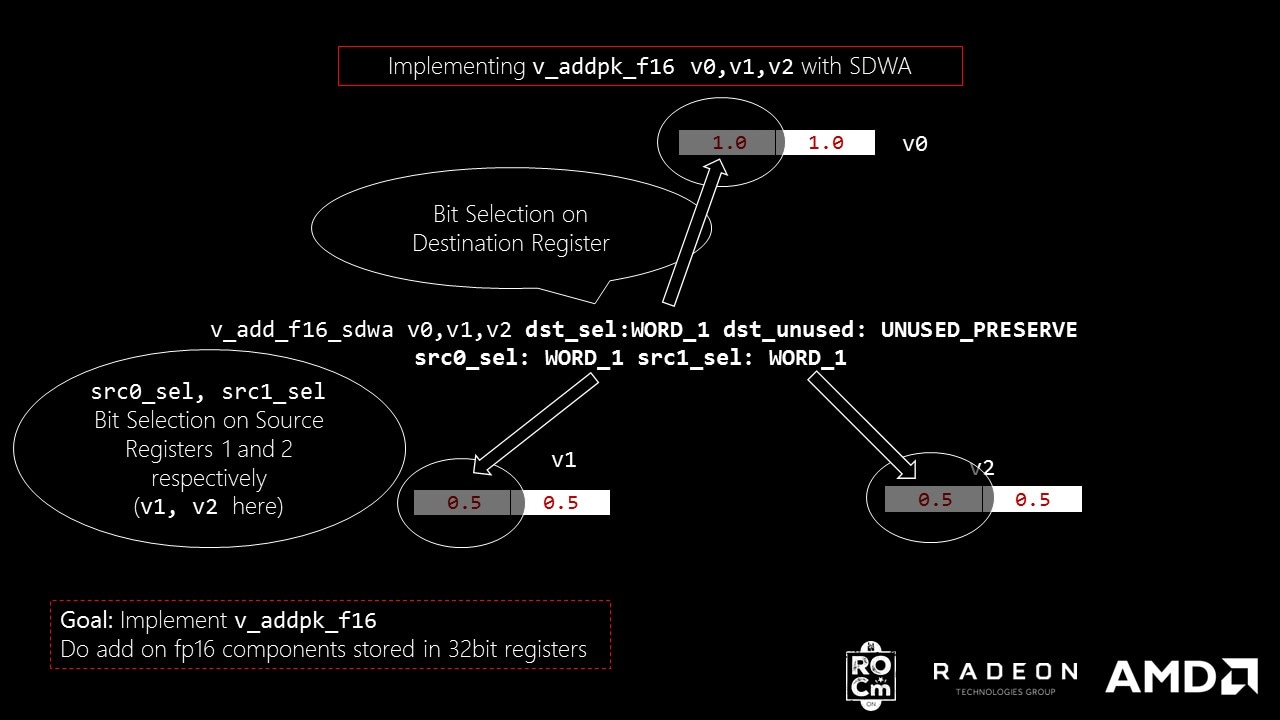
Using SDWA, a 16-bit float addition using the most significant part of a 32-bit register can be accomplished as follows:
v_add_f16_sdwa v0, v1, v2 dst_sel:WORD_1 dst_unused:UNUSED_PRESERVE src0_sel:WORD_1 src1_sel:WORD_1
v_add_f16_sdwa
mean that we are operating add op on 2 16bit floats in SDWA mode.dst_sel:WORD_1
mean that we are storing the output in [31:16] of v0
(WORD_1, [15:0] means WORD_0).dst_unused:UNUSED_PRESERVE
mean that the rest of the bits after storing in output will not be made 0. Which means with the current instruction, [15:0] bits of v0
are left untouched.src0_sel:WORD_1
mean that we are using [31:16] of v1
as inputsrc1_sel:WORD_1
mean that we are using [31:16] of v2
as input
The size of this instruction is only 64-bit (8bytes) and has 1x the execution rate of v_add_f16
. Using SDWA saves instruction cache misses and the ALU can operate at full op rate. No extra registers used, there is no drop in rate and only 4 bytes are added instruction cache.
Example
In several Machine Learning algorithms, training the data on fp16
data types has been effective in increasing the execution rate. In some cases the amount of training data is reduced to half and the effective bandwidth is improved by 2. Of greatest interest is optimizing the most used fp16
ops in a kernel, add, mul, mad
. This example shows an implementation of v_addpk_f16
that does a component-wise add on 2 fp16s loaded into a 32-bit register.
v_addpk_f16
# v_addpk_f16 v1, v2, v3
v_add_f16 v1, v2, v3
v_add_f16_sdwa v1, v2, v3 dst_sel:WORD_1 dst_unused:UNUSED_PRESERVE src0_sel:WORD_1 src1_sel:WORD_1
That’s all it takes and the rate of the instructions does not change, which means you get the same TFLOPs as a v_add_f16
. Also, this piece of code takes 32 + 64 bits on instruction cache (12 bytes). dst_unused:UNUSED_PRESERVE
means that the data present in WORD_0
is not touched (hence the word PRESERVE).
The next example is an implementation of v_madpk_f16
, and shows the limitations of SDWA.
v_madpk_f16
# v_madpk_f16 v1, v2, v3, v4
v_mad_f16 v1, v2, v3, v4
v_mul_f16_sdwa v1, v2, v3 dst_sel:WORD_1 dst_unused:UNUSED_PRESERVE src0_sel:WORD_1 src1_sel:WORD_1
v_add_f16_sdwa v1, v1, v4 dst_sel:WORD_1 dst_unused:UNUSED_PRESERVE src0_sel:WORD_1 src1_sel:WORD_1
Wait! Why not use v_mad_f16_sdwa
? Because v_mad_f16
is already a 64-bit encoded instruction ( vop3
); it isn’t one of the instructions that supports Sub-DWord addressing: vopc, vop1, vop2
. In other words, SDWA doesn’t apply here. Eventhough v_mac_f16
is a 32bit encoded instruction (vop2), it only allows DWORD addressing for destination register.
One More?
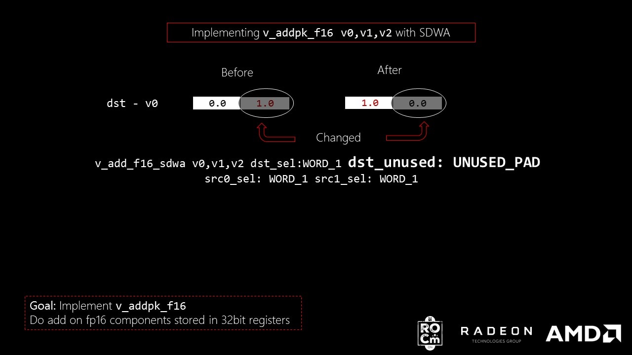
Let’s try one more example swapping the results between the most significant part and least significant part of a packed add before storing it in destination register?
# v_addpk_swap_f16 v0, v1, v2
v_add_f16_sdwa v0, v1, v2 dst_sel:WORD_1 dst_unused:UNUSED_PAD src0_sel:WORD_0 src1_sel:WORD_0
v_add_f16_sdwa v0, v1, v2 dst_sel:WORD_0 dst_unused:UNUSED_PRESERVE src0_sel:WORD_1 src1_sel:WORD_1
or
# v_addpk_swap_f16 v0, v1, v2
v_add_f16_sdwa v0, v1, v2 dst_sel:WORD_0 dst_unused:UNUSED_PAD src0_sel:WORD_1 src1_sel:WORD_1
v_add_f16_sdwa v0, v1, v2 dst_sel:WORD_1 dst_unused:UNUSED_PRESERVE src0_sel:WORD_0 src1_sel:WORD_0
Performance
SDWA operations seem nice, but how do they perform and how do you use them? In HIP, several SDWA math operations are implemented using the techniques described in this blog. A full list can be found here Link.
HIP is a portable higher level API that has similar syntax as CUDA which works on both AMD and NVIDIA GPUs. Module APIs from HIP can be utilized to load and run AMD GPU HSA code objects compiled offline. Using HIP several performance tests using the SDQA math operations were created, using the following techniques:
- The kernels for performance test were written in LLVM IR.
- LLVM (which is open source and fully supported by ROCm) was used to compile IR to AMD GCN ISA.
- CLANG was used to compile ISA to a HSA Code Object
- Finally, the HIPs Module API loaded the code object and ran the kernel using
hipModuleLaunchKernel.
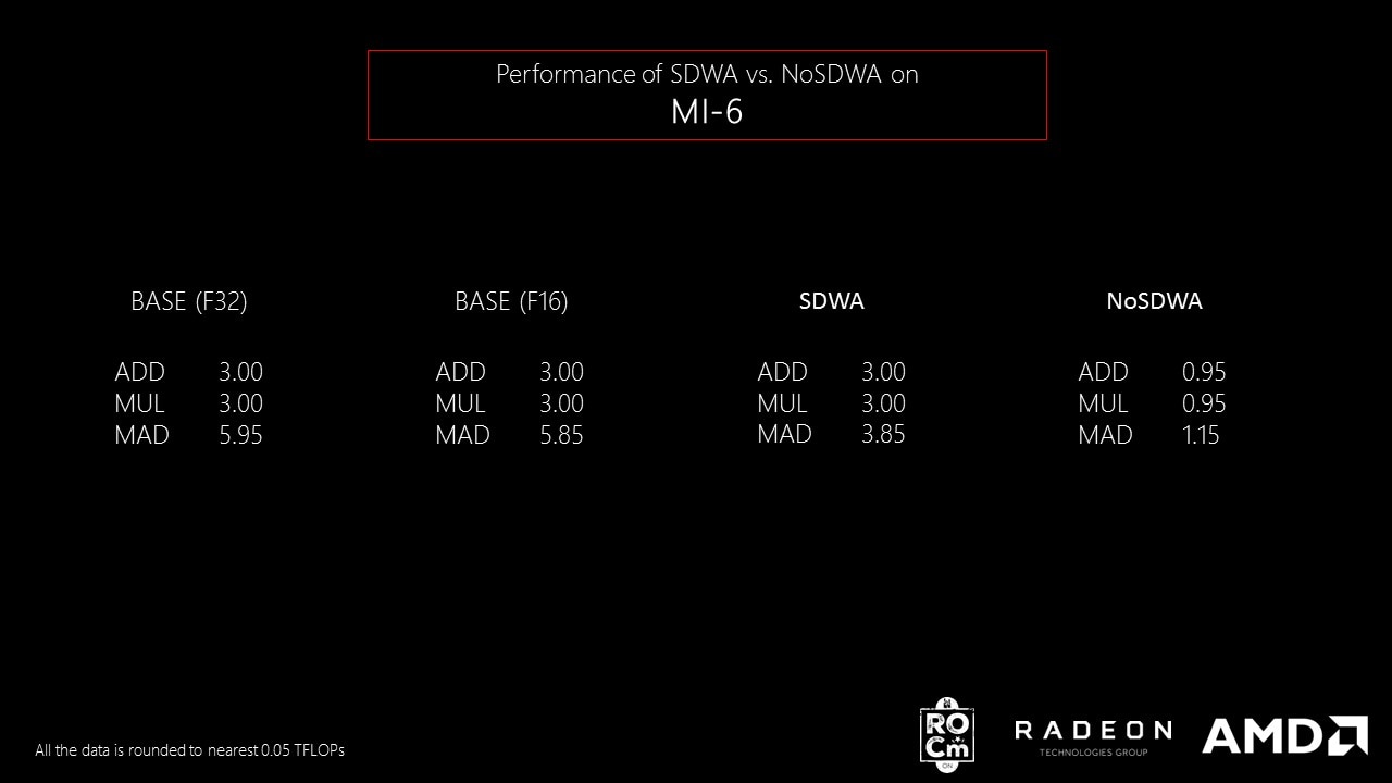
Generating AMD GCN ISA is important as it helps to check whether we are generating the ISA we intend to benchmark. MI-6 and MI-8 cards which are gfx8 cards were used to generate performance numbers. The following table presents the results:
The numbers in the above image show that v_addpk_f16
performs same as v_add_f16
on MI-6 and MI-8 using SDWA. The non-SDWA implementation is 0.25x or 0.3x the performance of v_add_f16
. v_madpk_f16
cannot achieve same performance as v_mad_f16
as it cannot operate on most significant 32 bit register using SDWA. Hence only a fraction of v_mad_f16
throughput is achieved.


