


Cross-lane operations are an efficient way to share data between wavefront lanes. This article covers in detail the cross-lane features that GCN3 offers. I’d like to thank Ilya Perminov of Luxsoft for co-authoring this blog post.
Terminology
We’ll be optimizing communication between work-items, so it is important to start with a consistent set of terminology:
- The basic execution unit of an AMD GCN GPU is called a wavefront, which is basically a SIMD vector.
- A wavefront comprises 64 parallel elements, called lanes, that each represent a separate work item.
- A lane index is a coordinate of the work item in a wavefront, with a value ranging from 0 to 63.
- Because a wavefront is the lowest level that flow control can affect, groups of 64 work items execute in lockstep. The actual GCN hardware implements 16-wide SIMD, so wavefronts decompose into groups of 16 lanes called wavefront rows that are executed on 4 consecutive cycles.
This hardware organization affects cross-lane operations – some operations work at the wavefront level and some only at the row level. We’ll discuss the details below.
Why Not Just Use LDS?
Local data share (LDS) was introduced exactly for that reason: to allow efficient communication and data sharing between threads in the same compute unit. LDS is a low-latency RAM physically located on chip in each compute unit (CU). Still, most actual compute instructions operate on data in registers. Now, let’s look at the peak-performance numbers. The memory bandwidth of AMD’s Radeon R9 Fury X is an amazing 512 GB/s. Its LDS implementation has a total memory bandwidth of (1,050 GHz) * (64 CUs) * (32 LDS banks) * (4 bytes per read per lane) = 8.6 TB/s. Just imagine reading all the content of a high-capacity 8 TB HDD in one second! Moreover, the LDS latency is an order of magnitude less than that of global memory, helping feed all 4,096 insatiable ALUs. LDS is only available on a workgroup level.
At the same time, the register bandwidth is (1,050 GHz) * (64 CUs) * (64 lanes) * (12 bytes per lane) = 51.6 TB/s. That’s another order of magnitude, so communication between threads is much slower than just crunching data in the thread registers.
But can we do better by sharing? The answer is yes, if we further reduce our scope from a workgroup to a single wavefront.
DS-Permute Instructions
As a previous post briefly described, GCN3 includes two new instructions: ds_permute_b32
and ds_bpermute_b32
. They use LDS hardware to route data between the 64 lanes of a wavefront, but they don’t actually write to an LDS location. These instructions don’t require pairing; they simply provide a different way to express the lane addressing. The ds_permute_b32
instruction implements forward permute (“push” semantics), or simply “put my data in lane i,” and ds_bpermute_b32
(note the letter ‘b’ before permute
) implements backward permute (“pull” semantics), or “read data from lane i.” They have the following syntax:
ds_permute_b32 dest, addr, src [offset:addr_offset] // push to dest
ds_bpermute_b32 dest, addr, src [offset:addr_offset] // pull from src

// Examples:
ds_permute_b32 v0, v1, v2
ds_bpermute_b32 v0, v0, v1 offset:0x10
where dest, addr
and src
are VGPRs (vector general purpose registers) and addr_offset
is an optional immediate offset. Both instructions take data from src
, shuffle it on the basis of the provided address ( addr + addr_offset
) and save it to the dest
register. The whole process divides into two logical steps:
- All active lanes write data to a temporary buffer.
- All active lanes read data from the temporary buffer, with uninitialized locations considered to be zero valued.
Addressing in Permute Instructions
The permute instructions move data between lanes but still use the notion of byte addressing, as do other LDS instructions. Hence, the value in the addr
VGPR should be desired_lane_id * 4
, since VGPR values are 4 bytes wide.
The instructions add the addr_offset
immediate to the addr
value before accessing the temporary buffer, and this immediate can be used to rotate src
values. Note that the instructions require a byte address, but they only move fully aligned doublewords. To put it another way, they only use bits [7:2] of the final address.
In many cases, the permute address is based on a work-item ID or lane ID. The work-item ID is loaded into v0
(and possibly v1
and v2
for multidimensional groups) before kernel execution. If you need the lane ID, try the following code, which fills VGPR v6
with that ID:
v_mbcnt_lo_u32_b32 v6, -1, 0
v_mbcnt_hi_u32_b32 v6, -1, v6
Backward-Permute Example
Consider the following ds_bpermute_b32
example with a simplified eight-lane wavefront; the VGPRs appear in yellow, the temporary buffer ( tmp
) in pink and inactive lanes in gray.
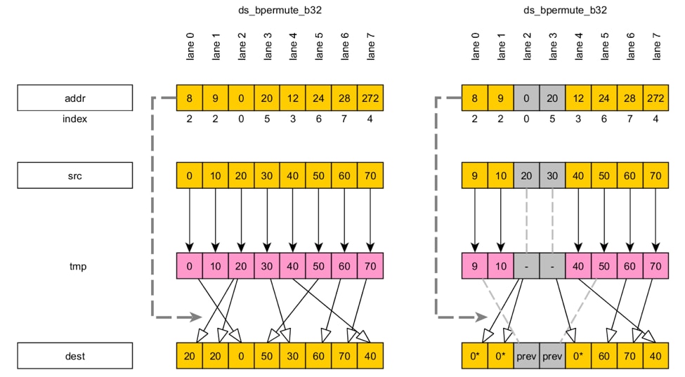
In the first step, all lanes write data from src
to corresponding locations in tmp
. In the second step, they all read data from the tmp
buffer on the basis of the address in addr
. The index
number shows the actual index of the tmp
element from the second step. As the figure above illustrates, addr
values in lanes 0 and 1 are different. Both values point to the same tmp
element, however, because the two least-significant address bits are ignored. Similarly, address 272 in lane 7 wraps around and points to element 4 in the src
register.
The right side of the figure shows an example using the same argument values but with the EXEC
mask disabling lanes 2 and 3. As a result, the instruction won’t overwrite the dest
elements corresponding to those lanes. Moreover, some lanes read from uninitialized tmp
elements and thus receive a zero value.
Forward-Permute Example
Now consider a ds_permute_b32
example using the same arguments as before:
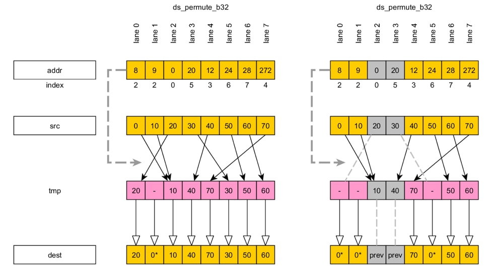
All lanes write src
data to the tmp
buffer on the basis of the addresses in the addr
register, followed by a direct read in the second step. Everything else here is the similar to the first example, with one exception: some lanes can write to the same tmp
element (consider lanes 0 and 1 in the figure above). Such a situation is impossible in the case of ds_bpermute_b32
. This conflict is resolved in the same way as writing to the same LDS address: the lane with the greater ID wins.
The Swizzle Instruction
The ds_swizzle_b32
instruction allows lanes to exchange their data in some limited ways. The advantage relative to permute instructions is that ds_swizzle_b32
requires no additional VGPR—the swizzle pattern is encoded in the instruction’s offset field. Moreover, this feature will most likely save a few address generation instructions required for ds_permute
. The swizzle instruction has the following syntax:
ds_swizzle_b32 dest, src offset:ds_pattern
// Examples:
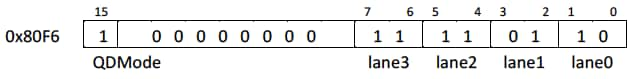
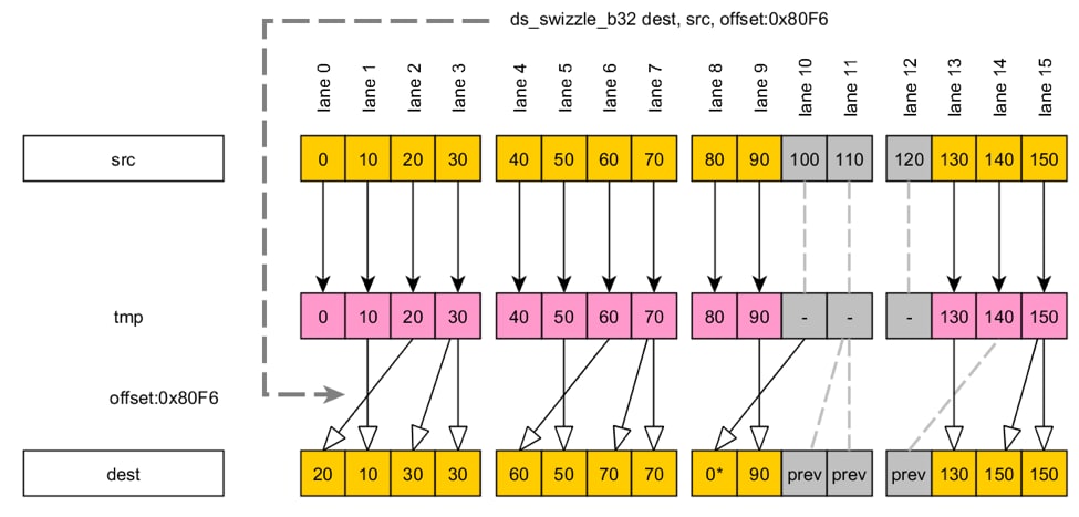
ds_swizzle_b32 v5, v2 offset:0x80F6
A ds_swizzle_b32
implements “pull” semantics: each lane reads some element of src
. The EXEC
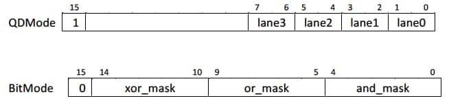
mask functions in the same way as in the case of the permute instructions. The 15th bit of ds_pattern
controls which of the two modes will be used:
- Quad-permute mode (QDMode). Each of the four adjacent lanes can access each other’s data, and the same switch applies to each set of four. The
ds_patternLSBs directly encode the element ID for each lane. - Bit-masks mode (BitMode). This mode enables limited data sharing within 32 consecutive lanes. Each lane applies bitwise logical operations with constants to its lane ID to produce the element ID from which to read. Constants are encoded in
ds_pattern.
The diagram below shows the ds_pattern
layout for each mode:
Consider the formal ds_pattern
description:
// QDMode - full data sharing in 4 consecutive threads
if (offset[15]) {
     for (i = 0; i < 32; i+=4) {
          thread_out[i+0] = thread_valid[i+offset[1:0]] ? thread_in[i+offset[1:0]] : 0;
          thread_out[i+1] = thread_valid[i+offset[3:2]] ? thread_in[i+offset[3:2]] : 0;
          thread_out[i+2] = thread_valid[i+offset[5:4]] ? thread_in[i+offset[5:4]] : 0;
          thread_out[i+3] = thread_valid[i+offset[7:6]] ? thread_in[i+offset[7:6]] : 0;
     }
}

// BitMode - limited data sharing in 32 consecutive threads
else {
     and_mask = offset[4:0];
     or_mask = offset[9:5];
     xor_mask = offset[14:10];
     for (i = 0; i < 32; i++)
     {
         j = ((i & and_mask) | or_mask) ^ xor_mask;
         thread_out[i] = thread_valid[j] ? thread_in[j] : 0;
     }
}
// Same shuffle applied to the second half of wavefront
QDMode is clear, as the following example illustrates:
On the other hand, BitMode looks more complicated; and_mask
, or_mask
and xor_mask
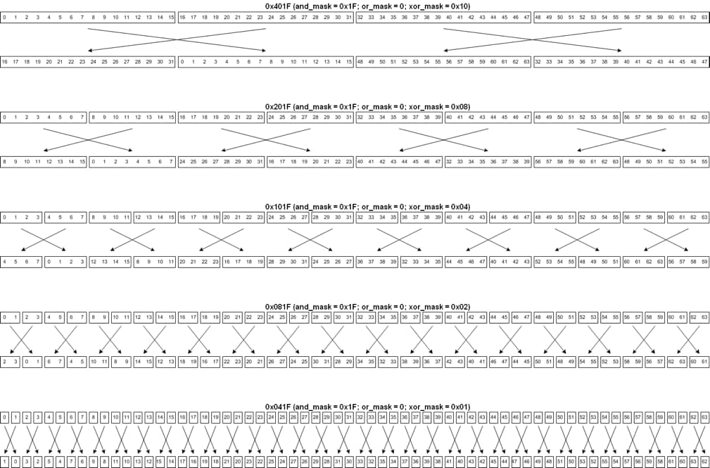
apply sequentially to the lane index, as the code above shows. By setting these masks, you can choose one of the operations applied to each bit of the lane index: set to 0, set to 1, preserve or inverse. Some of the interesting patterns are the following:
Swap the neighboring groups of 1, 2, 4, 8 or 16 lanes ( and_mask = 0x1F
, or_mask = 0x0
and only one bit is set in xor_mask
):
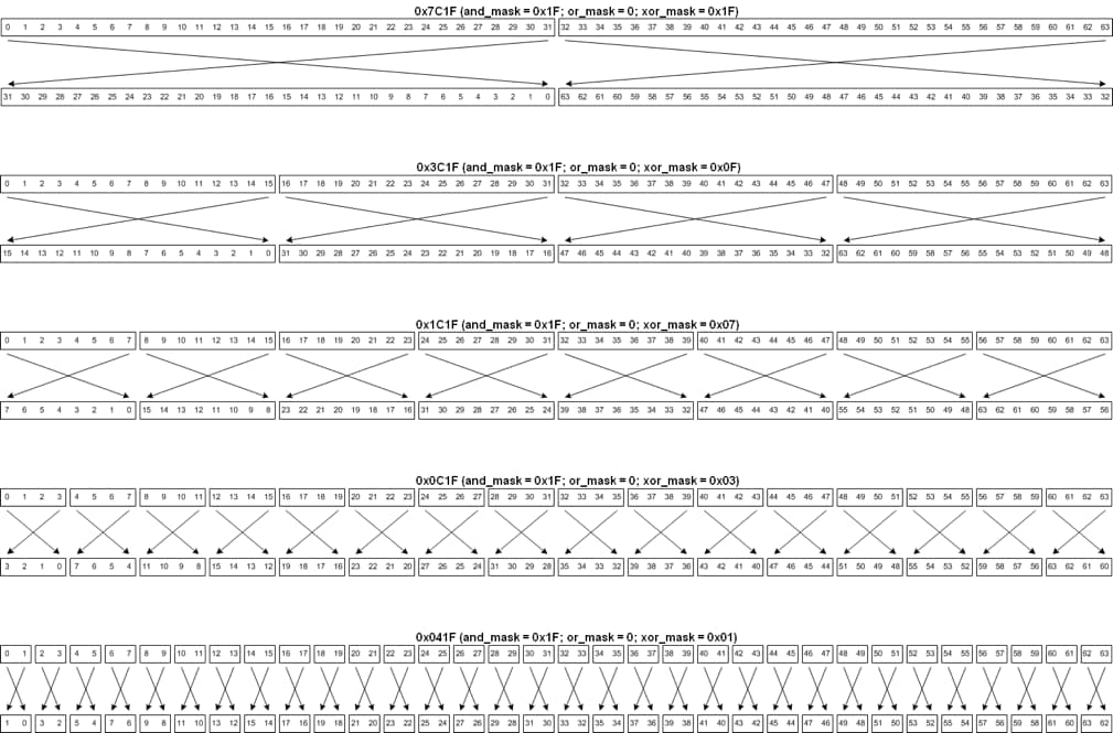
Mirror/reverse the lanes for groups of 2, 4, 8, 16 or 32 lanes ( and_mask = 0x1F, or_mask = 0x0
and the LSBs of xor_mask
are set to 1):
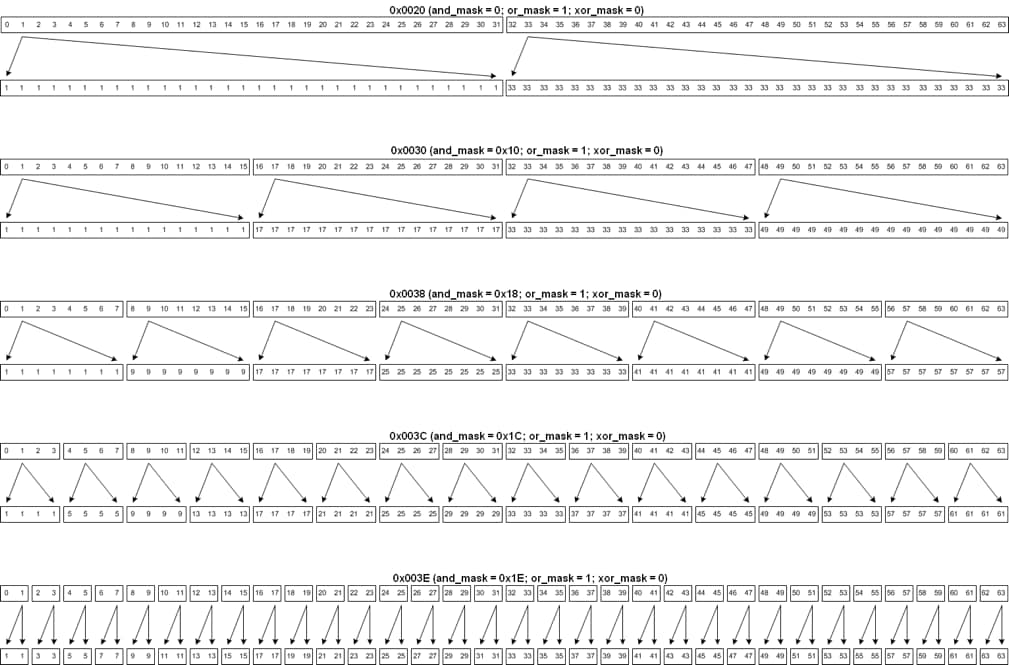
Broadcast the value of any particular lane for groups of 2, 4, 8, 16 or 32 lanes ( and_mask
MSBs are 1 and LSBs are 0, or_mask
is the lane index for a group, and xor_mask = 0x0
):
Other Notes on DS Cross-Lane Instructions
The permute and swizzle instructions employ LDS hardware. Thus, you must use s_waitcnt
to determine when data is returned to the destination VGPR. Such an approach, however, has many advantages compared with manually passing data using LDS memory:
- The permute and swizzle instructions don’t access LDS memory and may be called even if the wavefront has no allocated LDS memory.
- The approach requires only one instruction, not
ds_write*andds_read*, so it executes faster and saves space in the instruction cache. - It avoids LDS-bank conflicts for an arbitrary shuffle, so instructions have low latency.
Data-Parallel Primitives (DPP)
Now it’s time to talk about something really cool! The DPP feature doesn’t employ new instructions; rather, it introduces the new VOP_DPP
modifier, which allows VALU instructions to access data in neighboring lanes. Spending additional instruction to move data (even with the swizzle and permutes) is unnecessary—now, most of the vector instructions can do cross-lane reading at full throughput.
Of course, there’s no magic, so this feature only supports limited data sharing. DPP was developed with scan operations in mind, so it enables the following patterns (the corresponding DPP keywords appear in brackets):
- Full crossbar in a group of four (
quad_perm) - Wavefront shift left by one lane (
wave_shl) - Wavefront shift right by one lane (
wave_shr) - Wavefront rotate right by one lane (
wave_ror) - Wavefront rotate left by one lane (
wave_rol) - Row shift left by 1–15 lanes (
row_shl) - Row shift right by 1–15 lanes (
row_shr) - Row rotate right by 1–15 lanes (
row_ror) - Reverse within a row (
row_mirror) - Reverse within a half-row (
row_half_mirror) - Broadcast the 15th lane of each row to the next row (
row_bcast) - Broadcast lane 31 to rows 2 and 3 (
row_bcast)
Here, the term row means one-quarter of a wavefront (more on this subject later). The VOP_DPP
modifier can work with any VOP1
or VOP2
instruction encoding (the VOP3
and VOPC
encodings are unsupported), except the following:
-
v_clrexcp -
v_readfirstlane_b32 -
v_madmk_{ f16,f32} -
v_madak_{ f16,f32} -
v_movrel*_b32 - Instructions with 64-bit operands
The DPP modifier is encoded as a special 32-bit literal (search for VOP_DPP
in the GCN ISA guide), and this modifier always applies to the src0
instruction operand. The following example shows how to apply DPP to a particular instruction:
v_and_b32 dest, src0, src1 wave_shr:1
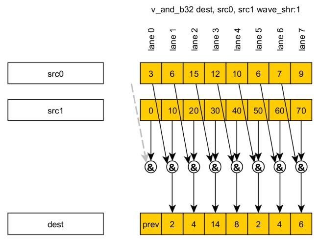
DPP Bound Control and Masking
As the example above shows, lane 0 should read from an invalid location (lane –1); hence, it fails to update its corresponding element in the dest
register. Alternatively, by setting the DPP-flag bound_ctrl:0
user can read 0 instead of disabling a lane (note that this is legacy notation; the bound_ctrl:0
flag will set the BOUND_CTRL
field of VOP_DPP
to 1). Lanes disabled by the EXEC
mask are also invalid locations from which to read values.
The lanes of a wavefront are organized in four banks and four rows, as the table below illustrates:
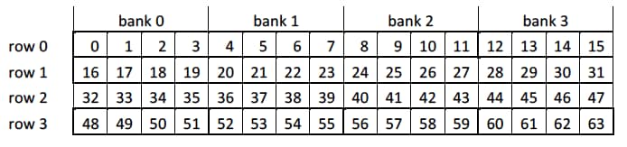
By setting row_mask
and bank_mask
, you can disable any bank or row in addition to the EXEC
mask, which is helpful for scan operations. As a quick summary:
- Lanes disabled by the
EXECmask or DPP mask will not update thedestregister. - Lanes that try to access invalid locations or data from lanes disabled by the
EXECmask- will not update the dest register if
BOUND_CTRL=0(default). - will read 0 as an
src0input ifBOUND_CTRL=1(DPP flagbound_ctrl:0).
- will not update the dest register if
DPP Example
Consider the following example, which computes a full prefix sum in a wavefront:
v_add_f32 v1, v0, v0 row_shr:1 bound_ctrl:0 // Instruction 1
v_add_f32 v1, v0, v1 row_shr:2 bound_ctrl:0 // Instruction 2
v_add_f32 v1, v0, v1 row_shr:3 bound_ctrl:0 // Instruction 3
v_nop // Add two independent instructions to avoid a data hazard
v_nop
v_add_f32 v1, v1, v1 row_shr:4 bank_mask:0xe // Instruction 4
v_nop // Add two independent instructions to avoid a data hazard
v_nop
v_add_f32 v1, v1, v1 row_shr:8 bank_mask:0xc // Instruction 5
v_nop // Add two independent instructions to avoid a data hazard
v_nop
v_add_f32 v1, v1, v1 row_bcast:15 row_mask:0xa // Instruction 6
v_nop // Add two independent instructions to avoid a data hazard
v_nop
v_add_f32 v1, v1, v1 row_bcast:31 row_mask:0xc // Instruction 7
The full code is available at GitHub (see dpp_reduce
in examples/gfx8
). Here, source data resides in v0
and the computed prefix sum in v1
. The following image shows data transfers for the above code:
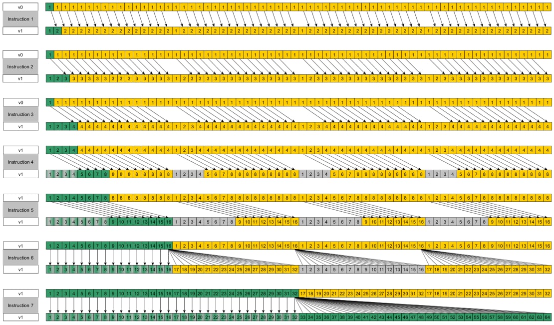
Lanes containing the final result appear in green, and lanes disabled by the DPP mask are in gray. The DPP masks from instructions 4 and 5 in the code above are optional and leave the result unaffected, because disabled lanes are effectively reading from invalid locations anyway. But the row_mask
parameter is necessary for instructions 6 and 7; otherwise, instruction 6 will corrupt values for lanes [0:15] and [32:47] and instruction 7 will corrupt values for lanes [0:31].
Other Notes on DPP Usage
The hardware resolves most data dependencies, but the software must handle a few cases explicitly to prevent data hazards. The full list of such cases is in the “Manually Inserted Wait States” section of the GCN ISA guide. For example, a sequence in which a VALU instruction updates an SGPR and a VMEM operation subsequently reads that SGPR is illegal. At least five so-called wait states must sit between these two operations. A wait state is a NOP or any other independent instruction.
Although DPP instructions execute at the full rate, they introduce new data-hazard sources that should be handled in software:
- If a previous VALU instruction modifies a VGPR read by DPP, two wait states are required. Note that this hazard affects only the operand that DPP reads. Consider instructions 2 and 3 in the example above; they consume the output from the previous VALU instruction by reading
v1. But DPP applies tov0, and becausev0is unmodified, wait states are unnecessary. - If a previous VALU instruction writes an
EXECmask, five wait states are required. This hazard is unlikely to become a problem because it’s triggered only by VALU instructions that write anEXECmask (anyv_cmpx_*, such asv_cmpx_ge_i32), and because scalar instructions are unaffected.
The DPP literal also has negative- and absolute-input modifiers, so such operations on float input values are free:
v_add_f32 v0, -v1, |v2| wave_shr:1
v_add_f32 v0, -|v1|, v2 wave_shr:1
Compiler and Tool Support
These new instructions can be accessed from HCC compiler or from the GCN assembler:
- AMD’s HCC compiler provides intrinsic function support for ds_permute, ds_bpermute, and ds_swizzle. These are device functions (marked with [[hc]]) and thus can be called from HC or HIP kernels (running on hcc):
-
extern "C" int __amdgcn_ds_bpermute(int index, int src) [[hc]]; -
extern "C" int __amdgcn_ds_permute(int index, int src) [[hc]]; -
extern "C" int __amdgcn_ds_swizzle(int src, int pattern) [[hc]];
-
- Additionally, DPP is exposed as a special move instruction. The compiler will combine the DPP move with the subsequent instructions, if possible:
-
extern "C" int __amdgcn_move_dpp(int src, int dpp_ctrl, int row_mask, int bank_mask, bool bound_ctrl) [[hc]];
When using these instrinsics, HCC will automatically ensure that the proper .waitcnt and data dependencies are honored.
- AMD also provides an open-source GCN assembler, integrated into the popular LLVM compiler. The GCN assembler includes support for all of the operations described here today, as well as full examples showing use of the instructions.
Summary
The table below provides notes summarizing our description of the DPP modifier and LDS-based instructions that provide cross-lane data-sharing capabilities.

AMD GPU Services (AGS) Library
The AMD GPU Services (AGS) library provides software developers with the ability to query AMD GPU software and hardware state information that is not normally available through standard operating systems or graphics APIs.

The Art of AMDGCN Assembly: How to Bend the Machine to Your Will
This article explains how to produce Hsaco from assembly code and also takes a closer look at some new features of the GCN architecture.
Using Sub DWord Addressing on AMD GPUs
Sub DWord Addressing is a feature of the AMD GCN architecture which allows the efficient extraction of 8-bit and 16-bit values from a 32-bit register.

AMD ISA Documentation
Instruction Set Architecture (ISA) documentation provides a guide for directly accessing the hardware.