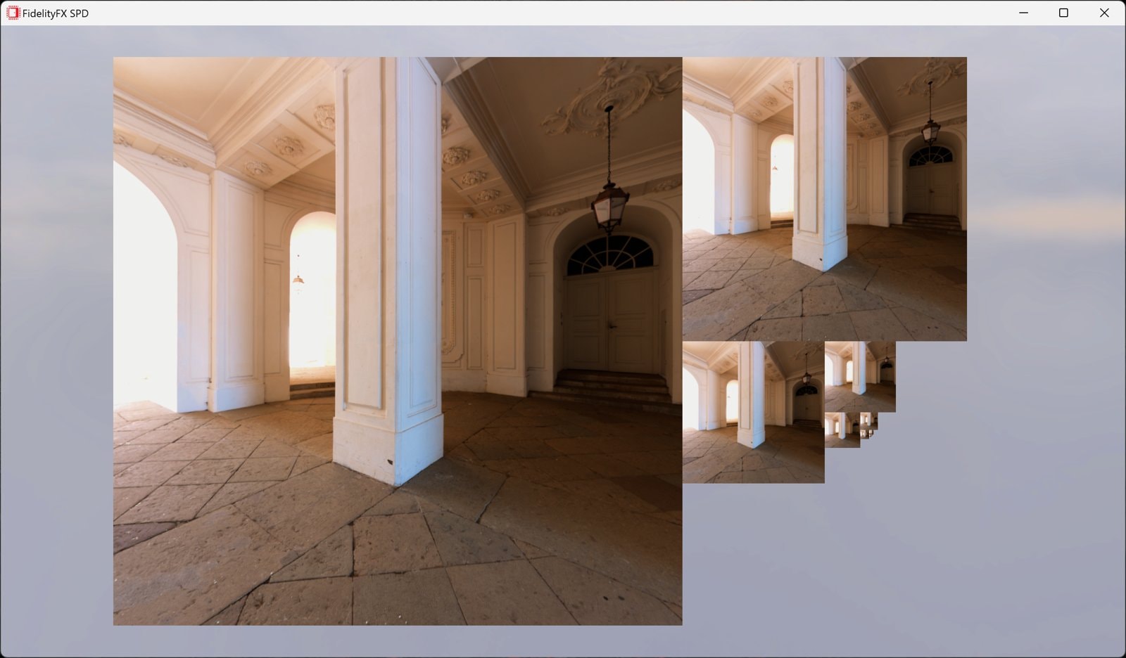
AMD FidelityFX™ Single Pass Downsampler (SPD)
AMD FidelityFX Single Pass Downsampler (SPD) provides an AMD RDNA™ architecture optimized solution for generating up to 12 MIP levels of a texture.
This post describes how GCN hardware coalesces memory operations to minimize traffic throughout the memory hierarchy. The post uses the term “invocation” to describe one shader invocation. This term is also commonly referred to as “lane” (as in one lane of a SIMD vector, or wave), and also “thread” (as in one thread of execution of a shader).
Reviewing peak throughput limits for a GCN Compute Unit (CU),
The one 2×2 fragment quad per clock rate provides hints about peak throughput. It takes up to 4 reads per fragment to gather the texels required for one filtered output, for a total of 16 reads for the 2×2 fragment quad per clock. Peak rate of one filtered 2×2 fragment quad per clock requires a return of 16 32-bit values in a single cycle (4 fragments * 4 channels). GCN leverages those two data paths to provide support for single channel buffer loads, in the cases described later in this post, at a rate of up to 16 32-bit values in a single cycle.
The peak rate of one 2×2 fragment quad per clock requires address generation for image VMEM operations for 4 invocations in one clock. For point sampled (non-filtered) image operations GCN can return results for up to four 128-bit texels per clock. For filtered image operations, GCN processes 32-bits for each four fragments per clock. So the same four 128-bit texels for filtered VMEM operations takes 4 clocks.
Summary of peak throughput per wave supported by data paths (actual rates will vary),
For L2 cache accesses, the hardware groups the accesses for all 64 invocations of a wave into the fewest 64-byte aligned 64-byte memory requests. For loads and stores, all accesses to any given aligned 64-byte cacheline get coalesced into a single memory request. Also note for stores, when multiple invocations of a wave write to the same address, they are automatically collapsed into one write to the given address. There is no need to waste VALU cycles to avoid colliding writes. This is not true for atomics, as each access to a given address must remain a unique operation.
Image VMEM operations are serviced in aligned groups of 4 invocations in a wave. For example in compute, invocations 3 would be a group, and in fragment or pixel shaders each 2×2 fragment quad is a group. Note compute invocations are organized in linear order: invocationIndex=x+(widthy)+(widthheight*z).
Multi-channel buffer VMEM operations, and buffer VMEM operations with single-channel accesses greater than 32-bits, are handled like point sampled image operations (as described above). Under specific cases, 32-bit (and smaller) single-channel buffer VMEM operations are first coalesced in aligned groups of 16 invocations in a wave. Invocations -15, -15, -15, and -15 are all separate groups. Cases include: